- 您现在的位置:买卖IC网 > Sheet目录320 > DK-DEV-5SGXEA7N (Altera)KIT DEV STRATIX V FPGA 5SGXEA7
SV51008
2014.01.10
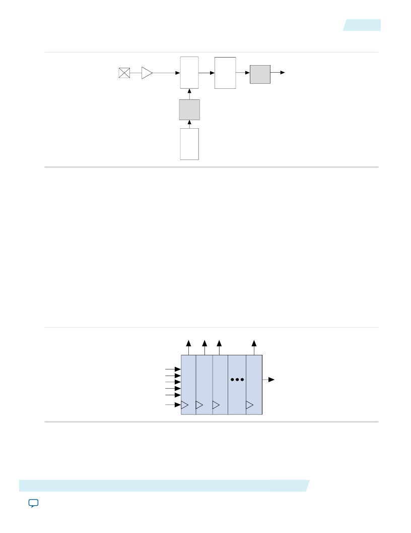
Figure 7-17: Delay Chains in the DQS Input Path
DQS
DQS delay
I/O and DQS Configuration Blocks
7-27
DQS
Enable
dqsin
chain
T7
delay
dqsbusout
chain
dqsenable
T11
delay
chain
DQS
Enable
Control
Related Information
Provides more information about programming the delay chains.
? DQS Delay Chain on page 7-20
I/O and DQS Configuration Blocks
The I/O and DQS configuration blocks are shift registers that you can use to dynamically change the settings
of various device configuration bits.
? The shift registers power-up low.
? Every I/O pin contains one I/O configuration register.
? Every DQS pin contains one DQS configuration block in addition to the I/O configuration register.
Figure 7-18: Configuration Block (I/O and DQS)
This figure shows the I/O configuration block and the DQS configuration block circuitry.
MSB
bit2
bit1
bit0
datain
update
ena
dataout
rankselectread
rankselectwrite
clk
Related Information
Provides details about the I/O and DQS configuration block bit sequence.
External Memory Interfaces in Stratix V Devices
Send Feedback
Altera Corporation
发布紧急采购,3分钟左右您将得到回复。
相关PDF资料
DK-DSP-2S180N
DSP PRO KIT W/SII EP2S180N
DK-DSP-3C120N
KIT DEV DSP CYCLONE III EDITION
DK-K7-CONN-CES-G
KINTEX-7 FPGA CONNECTIVITY KIT
DK-K7-EMBD-CES-G-J
KINTEX-7 FPGA EMBEDDED KIT JAPAN
DK-MAXII-1270N
KIT DEV MAXII W/EPM 1270N
DK-N2EVAL-3C25N
KIT DEV NIOS II CYCLONE III ED.
DK-NIOS-2C35N
NIOS II KIT W/CYCLONE II EP2C35N
DK-NIOS-2S60N
NIOS II KIT W/STRATIX II EP2S60N
相关代理商/技术参数
DK-DSP-2C70N
功能描述:DSP KIT W/CYCLONE II EPS2C70N RoHS:是 类别:编程器,开发系统 >> 通用嵌入式开发板和套件(MCU、DSP、FPGA、CPLD等) 系列:Cyclone® II 产品培训模块:Blackfin® Processor Core Architecture Overview
Blackfin® Device Drivers
Blackfin® Optimizations for Performance and Power Consumption
Blackfin® System Services 特色产品:Blackfin? BF50x Series Processors 标准包装:1 系列:Blackfin® 类型:DSP 适用于相关产品:ADSP-BF548 所含物品:板,软件,4x4 键盘,光学拨轮,QVGA 触摸屏 LCD 和 40G 硬盘 配用:ADZS-BFBLUET-EZEXT-ND - EZ-EXTENDER DAUGHTERBOARDADZS-BFLLCD-EZEXT-ND - BOARD EXT LANDSCAP LCD INTERFACE 相关产品:ADSP-BF542BBCZ-4A-ND - IC DSP 16BIT 400MHZ 400CSBGAADSP-BF544MBBCZ-5M-ND - IC DSP 16BIT 533MHZ MDDR 400CBGAADSP-BF542MBBCZ-5M-ND - IC DSP 16BIT 533MHZ MDDR 400CBGAADSP-BF542KBCZ-6A-ND - IC DSP 16BIT 600MHZ 400CSBGAADSP-BF547MBBCZ-5M-ND - IC DSP 16BIT 533MHZ MDDR 400CBGAADSP-BF548BBCZ-5A-ND - IC DSP 16BIT 533MHZ 400CSBGAADSP-BF547BBCZ-5A-ND - IC DSP 16BIT 533MHZ 400CSBGAADSP-BF544BBCZ-5A-ND - IC DSP 16BIT 533MHZ 400CSBGAADSP-BF542BBCZ-5A-ND - IC DSP 16BIT 533MHZ 400CSBGA
DK-DSP-2S180N
功能描述:DSP PRO KIT W/SII EP2S180N RoHS:是 类别:编程器,开发系统 >> 通用嵌入式开发板和套件(MCU、DSP、FPGA、CPLD等) 系列:Stratix® II 产品培训模块:Blackfin® Processor Core Architecture Overview
Blackfin® Device Drivers
Blackfin® Optimizations for Performance and Power Consumption
Blackfin® System Services 特色产品:Blackfin? BF50x Series Processors 标准包装:1 系列:Blackfin® 类型:DSP 适用于相关产品:ADSP-BF548 所含物品:板,软件,4x4 键盘,光学拨轮,QVGA 触摸屏 LCD 和 40G 硬盘 配用:ADZS-BFBLUET-EZEXT-ND - EZ-EXTENDER DAUGHTERBOARDADZS-BFLLCD-EZEXT-ND - BOARD EXT LANDSCAP LCD INTERFACE 相关产品:ADSP-BF542BBCZ-4A-ND - IC DSP 16BIT 400MHZ 400CSBGAADSP-BF544MBBCZ-5M-ND - IC DSP 16BIT 533MHZ MDDR 400CBGAADSP-BF542MBBCZ-5M-ND - IC DSP 16BIT 533MHZ MDDR 400CBGAADSP-BF542KBCZ-6A-ND - IC DSP 16BIT 600MHZ 400CSBGAADSP-BF547MBBCZ-5M-ND - IC DSP 16BIT 533MHZ MDDR 400CBGAADSP-BF548BBCZ-5A-ND - IC DSP 16BIT 533MHZ 400CSBGAADSP-BF547BBCZ-5A-ND - IC DSP 16BIT 533MHZ 400CSBGAADSP-BF544BBCZ-5A-ND - IC DSP 16BIT 533MHZ 400CSBGAADSP-BF542BBCZ-5A-ND - IC DSP 16BIT 533MHZ 400CSBGA
DK-DSP-2S60N
功能描述:DSP KIT W/STRATIX II EP2S60N RoHS:是 类别:编程器,开发系统 >> 通用嵌入式开发板和套件(MCU、DSP、FPGA、CPLD等) 系列:Stratix® II 产品培训模块:Blackfin® Processor Core Architecture Overview
Blackfin® Device Drivers
Blackfin® Optimizations for Performance and Power Consumption
Blackfin® System Services 特色产品:Blackfin? BF50x Series Processors 标准包装:1 系列:Blackfin® 类型:DSP 适用于相关产品:ADSP-BF548 所含物品:板,软件,4x4 键盘,光学拨轮,QVGA 触摸屏 LCD 和 40G 硬盘 配用:ADZS-BFBLUET-EZEXT-ND - EZ-EXTENDER DAUGHTERBOARDADZS-BFLLCD-EZEXT-ND - BOARD EXT LANDSCAP LCD INTERFACE 相关产品:ADSP-BF542BBCZ-4A-ND - IC DSP 16BIT 400MHZ 400CSBGAADSP-BF544MBBCZ-5M-ND - IC DSP 16BIT 533MHZ MDDR 400CBGAADSP-BF542MBBCZ-5M-ND - IC DSP 16BIT 533MHZ MDDR 400CBGAADSP-BF542KBCZ-6A-ND - IC DSP 16BIT 600MHZ 400CSBGAADSP-BF547MBBCZ-5M-ND - IC DSP 16BIT 533MHZ MDDR 400CBGAADSP-BF548BBCZ-5A-ND - IC DSP 16BIT 533MHZ 400CSBGAADSP-BF547BBCZ-5A-ND - IC DSP 16BIT 533MHZ 400CSBGAADSP-BF544BBCZ-5A-ND - IC DSP 16BIT 533MHZ 400CSBGAADSP-BF542BBCZ-5A-ND - IC DSP 16BIT 533MHZ 400CSBGA
DK-DSP-3C120N
功能描述:可编程逻辑 IC 开发工具 FPGA Development Kit For EP3C120F780
RoHS:否 制造商:Altera Corporation 产品:Development Kits 类型:FPGA 工具用于评估:5CEFA7F3 接口类型: 工作电源电压:
DK-DSP-3SL150N
功能描述:可编程逻辑 IC 开发工具 FPGA Development Kit For EP3SL150F1152
RoHS:否 制造商:Altera Corporation 产品:Development Kits 类型:FPGA 工具用于评估:5CEFA7F3 接口类型: 工作电源电压:
DK-DTK-120HW
制造商:FLORIDA MISC. 功能描述:
DKE10
制造商:MEANWELL 制造商全称:Mean Well Enterprises Co., Ltd. 功能描述:10W DC-DC Regulated Dual Output Converter
DKE10A-05
功能描述:DC/DC转换器 9-18Vin +/-5Vout 100-1000mA, 10W RoHS:否 制造商:Murata 产品: 输出功率: 输入电压范围:3.6 V to 5.5 V 输入电压(标称): 输出端数量:1 输出电压(通道 1):3.3 V 输出电流(通道 1):600 mA 输出电压(通道 2): 输出电流(通道 2): 安装风格:SMD/SMT 封装 / 箱体尺寸:
